Last time our compiler generated a few files but we only used the main.ihx one to flash the microcontroller. In this brief entry we are going to take a look at some other files to understand what is happening under the hood.
To begin with let’s quickly explain how the code is ran in the microcontroller.
Architecture
The very basic building blocks of a microcontroller or even a computer are the Central Processing Unit (CPU) and the Memory. The memory stores the data and the CPU processes it.
The CPU itself is composed of the Arithmetic Logic Unit (ALU), that performs arithmetic and logic operations, processor registers that supply operands to the ALU and store the results of its operations and the Control Unit (CU) that manages all the processes.
The different components are linked together by one or more Data Buses.
Computer Instructions
In order to make something to happen, hopefully what is written in our code, we need to tell the CPU where to get the data and how to process it. This is done using Instructions, which are a representation of a real physical process, you can think of them as the last frontier between firmware and hardware. They are an array of bits called operation code (OP code) composed of an identifier and some arguments that can be data or memory locations.
Instructions can be stored in the same memory as the data and the program (Von-Neumann Architecture), or in their independent memory (Harvard Architecture). Our STM8 uses a modified version of Harvard Architecture with a Reduced Instruction Set (RISC).
Program execution
When an instruction is called by the CU, the different data paths that connect the buses, ALU and memory registers are rearranged to perform the desired action, this is better explained with an example. Consider this oversimplified model of a microcontroller programmed to add the values of two variables (x and y) and store the result in a third one (z):
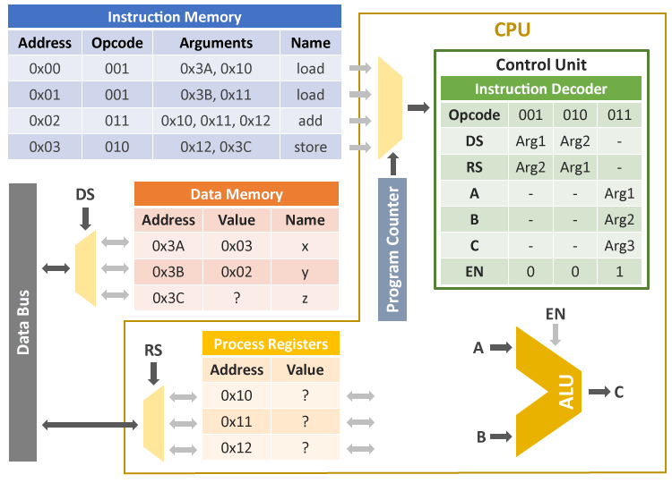
What we can see in the picture is the following:
- A memory that contains the instructions in the proper order
- A memory that stores the variables and their values
- A Program Counter (PC) that iterates over the instructions
- A Control Unit with an Instruction Decoder (The Instruction Set)
- The ALU with two inputs (A and B), one output (C) and an enable switch (EN)
- A Process Register bank
- The Parallel Data Bus that transmits the information
- Two “gates”, Data Select (DS) and Register Select (RS)
Next we go though the different steps of the program execution.
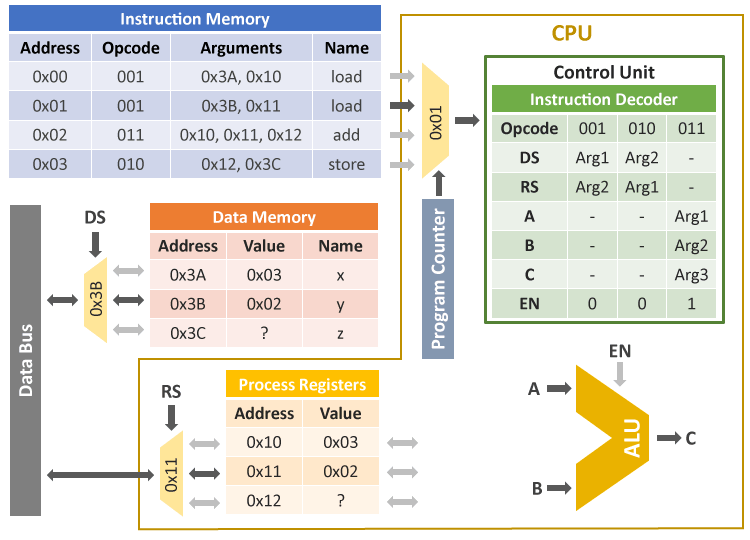
Step 1: Loading the value of “x”
 The program counter is at 0x00 and the instruction 0x00 (Load x) is passed to the
CU and decoded. After that the DS and RS gates are set according to the arguments
of the instruction and the value of 0x3A (x) is loaded into the register 0x10.
The program counter is at 0x00 and the instruction 0x00 (Load x) is passed to the
CU and decoded. After that the DS and RS gates are set according to the arguments
of the instruction and the value of 0x3A (x) is loaded into the register 0x10.
In our model this operation takes just 1 clock cycle (in a real case this can be different) and it happens almost immediately if we ignore the propagation delay of the hardware. Also we are making the assumption that the parallel bus is as wide as the registers so that the data can be copied in one go.
Step 2: Loading the value of “y”
 The program counter increases by one and the next instruction (0x01) is loaded
and the previous process is repeated.
The program counter increases by one and the next instruction (0x01) is loaded
and the previous process is repeated.
Step 3: Adding the values
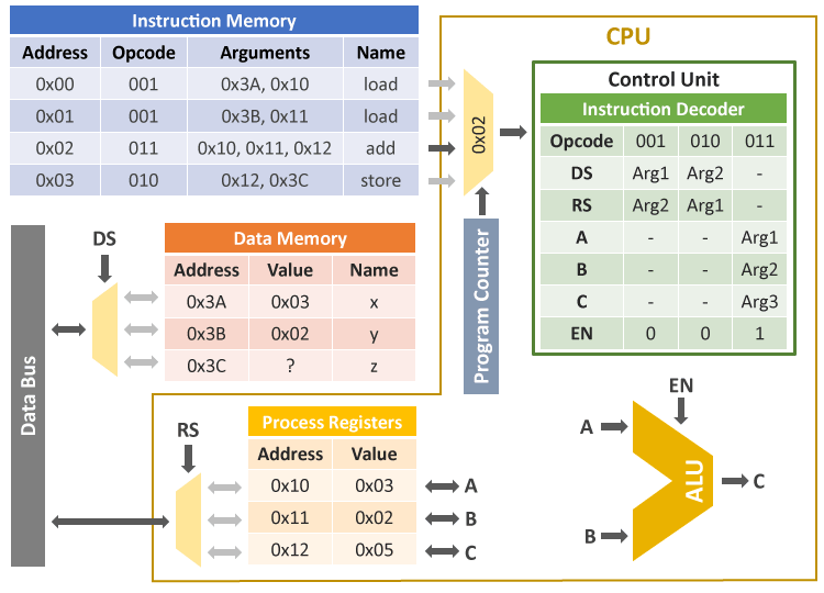 Next the Add instruction is executed. This time the data bus is not used, instead
the the process registers 0x10 and 0x11 are passed to the ALU and the
result is stored into the 0x12 register. In our case, the ALU can only perform addition,
so we only have to set the enable pin (EN) to perform the operation.
Next the Add instruction is executed. This time the data bus is not used, instead
the the process registers 0x10 and 0x11 are passed to the ALU and the
result is stored into the 0x12 register. In our case, the ALU can only perform addition,
so we only have to set the enable pin (EN) to perform the operation.
Step 4: Storing the result
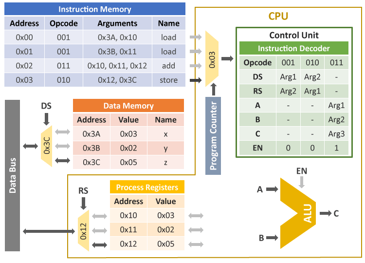 Finally the last instruction is executed and the result value stored in the process
register is copied to the memory.
Finally the last instruction is executed and the result value stored in the process
register is copied to the memory.
As you can see with this simple example the process is quite straight forward. Of course you have to take into account that a real microcontroller or computer is much more complex, and includes many more instructions to perform arithmetics, logic and conditional jumps… but this can serve as a good base to understand how things work.
The machine code
When we executed the compiler last time many files were generated including the main.asm file. The .asm extension stands for Assembly Language and it is a language that explicitly shows the instructions that compose a program in a format that a human can read.
In the main.asm file our blink code starts at the line 90. The lines prior to it are initializations for the microcontroller.
;main.c: 6: PB_DDR = (1 << 5);
	mov	0x5007+0, #0x20
;	main.c: 8: while(1){
00103$:
;main.c: 9: PB_ODR ^= (1 << 5);
	bcpl	20485, #5
;main.c: 10: for(int i = 0; i < 30000; i++){;}
	clrw	x
00106$:
	cpw	x, #0x7530
	jrsge	00103$
	incw	x
	jra	00106$
;main.c: 13: }
	ret
In this bit of code we can differentiate a few elements:
- Instructions (e.g.
clrw x) - Tags (e.g.
_main:or00106$:) - hex representation (e.g.
0082C 5F) - Comments (e.g.
;main-c: 8: while(1){)
Reading the assembly code
The comments give us a general idea of that is happening next, but we are going analyze the code in detail to understand it better. Keep in mind that as many other languages, this is executed from top to bottom line by line, furthermore I suggest you keeping the blink main.c code on hand and getting a copy of the the STM8 Programming Manual where you can find what the different instructions do. I guarantee the previous code already can be much clearer if you just understand the meaning of the acronyms.
Nevertheless, let’s begin:
_main:
This is an identifier tag for the main function. It is called at the after the initialization of the microcontroller.
;main.c: 6: PB_DDR = (1 << 5);
	mov	0x5007+0, #0x20
The mov (move) instruction takes two arguments, a memory address and a value. The
memory address is 0x5007+0 (PB_DDR) and the value (1 << 5) is directly converted to 0x20,
with the # meaning that is a numerical value. As you remember, we were not creating
any variable two first lines of the main.c files, and that is reflected in the assembly
code.
;main.c: 8: while(1){
00103$:
Another tag to indicate where the while loop starts.
;main.c: 9: PB_ODR ^= (1 << 5); // Toggle PB5
	bcpl	20485, #5
bcpl (Bit Complement) flips the nth bit of a memory address provided. In
this case the 5th bit of the memory address 20485 is flipped. Again, the address
is not arbitrary, converted to hex it is 0x5005 which is the address of the
PB_ODR.
Next the for loop structure starts and it’s composed of few lines.
;main.c: 10: for(int i = 0; i < 30000; i++){;}
	clrw	x
clrw (Clear word) clears the content of the process register x. More info about
the process registers can be found in the section 3.2 CPU registers of the
programming manual.
00106$:
	cpw	x, #0x7530
	jrsge	00103$
	incw	x
	jra	00106$
A tag is created and the cpw(Compare word) instruction compares the content of the
x register with 0x7530 (30000 in decimal) subtracting the two values. The N
(Negative) flag is set if the result is negative, the V (Overflow) flag is
set if the subtraction causes an overflow and the Z (Zero) flag is set when the result is 0.
More info about flags is available on the page 113 of the P.M.
Next the jrsge (Jump Relative if Signed Greater or Equal)
checks if the logic XOR
operation between N and V and jumps to the 00103$ tag if the result is 0.
But why the XOR of N and V has to be zero? I was trying to answer this question
for about a week, making binary subtractions, analyzing all the necessary bits but nothing
made much sense to me. Then I found this article that shows how a multi-bit comparator works, I recommend you checking it to understand why N and V flags are used.
The easiest explanation to our initial question (based on the article) is that XOR is used because
the “Greater or Equal” case is the complementary of the “Less” case, this being N XOR V = 1.
Basically we testing for x not being less than the specific value.
If we haven’t jumped to 00103$ the incw (Increase word) instruction is called and
the content of x is increased by one and the jra (Jump Relative Always) causes
the program to jump to the 00106$ tag.
In the end of the program we see a ret (Return from subroutine), which returns from
the main to the caller. However this instruction won’t be ever executed because
we are in an infinite while loop.
From assembly to hex
Once we understood our assembly code we can finally jump into the hex code that will be uploaded to our device. If we check the main.lst file, we can see that the hex is a direct translation from the assembly.
                               85 	.area CODE
                               86 ;	main.c: 4: void main(){
                               87 ;	-----------------------------------------
                               88 ;	 function main
                               89 ;	-----------------------------------------
000000                         90 _main:
                               91 ;	main.c: 6: PB_DDR = (1 << 5);
000000 35 20 50 07      [ 1]   92 	mov	0x5007+0, #0x20
                               93 ;	main.c: 8: while(1){
000004                         94 00103$:
                               95 ;	main.c: 9: PB_ODR ^= (1 << 5);
000004 90 1A 50 05      [ 1]   96 	bcpl	20485, #5
                               97 ;	main.c: 10: for(int i = 0; i < 30000; i++){;}
000008 5F               [ 1]   98 	clrw	x
000009                         99 00106$:
000009 A3 75 30         [ 2]  100 	cpw	x, #0x7530
00000C 2E F6            [ 1]  101 	jrsge	00103$
00000E 5C               [ 1]  102 	incw	x
00000F 20 F8            [ 2]  103 	jra	00106$
                              104 ;	main.c: 13: }
000011 81               [ 4]  105 	ret
In the section 7.4 Instruction Set of the P.M. we can identify all the OP codes of the instructions, let’s analyze, for example, the line 93 of the main.lst file:
000000 35 20 50 07 [ 1] 92 mov 0x5007+0, #0x20
We already know what this line does and now if we look at the OP code for the mov
instruction is easy to decode the hex bytes at the beginning of the line.
00000 is the address offset added to the base address which the .area Code indicates.
This base value (00008024) can be find in the main.map file.
Next we have 35 which is the identifier for the mov instruction. After that
we see the two arguments passed to instruction: the value to set 20 (#0x20) and
the location 50 (Most Significant) and 07 (Least Significant).

Finally we can take a look at the main.hex file:
:048000008200800773
:10800700AE00002707724F00005A26F9AE0000277E
:0D80170009D68023D700005A26F7CC80043C
:03800400CC802409
:1080240035205007901A50055FA375302EF65C205A
:02803400F881D1
:00000001FF
In the fifth line we see the previously analyzed line:
...80240035205007...
It is worth mentioning that some instructions don’t have the address explicitly indicated in the hex file. The length of the previous instruction serves as the address offset in that case. For example for the next instruction on the same line:
...901A5005...
the offset will be 000000 + 4 (length of mov) which is correct as you can see in
the main.lst code.
Here ends the basic introduction to assembly and hex, I hope now you have a better understanding of how your MCU works!